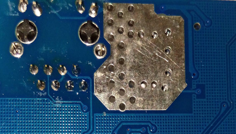
Definition
You might have heard this concept called “edge plating” or “castellation,” which is the copper plating that runs from the top to the bottom surfaces of a PCB, and runs along at least one of the perimeter edges. PCB edge castellation ensures a strong connection through the board and limits the chance of equipment failures, especially in controlling protections for small form factor boards and sub-motherboards.
Edge Plating PCB Process
Circuit board fabrication for edge soldering requires precision handling and faces many challenges around how plated edges are prepared and the lifetime adhesion of the plated material.
There are two standard ways to increase the growth of metal layers in circuit boards and holes:Line plating and full plate copper plating are described as follows:
1.Line Plating
This process only designed on circuit pattern and the hole where the copper layer is generated and etch resist metal plating.In the plating process, the width of each side of the circuit and pad is roughly the same as the thickness of the plating surface.Therefore, it is necessary to leave a margin on the original film.
Most of the copper surface in the line plating to be blocked by the agent, only plating on line and solder pad.
2.Full Plate Copper Plating
In this process, all the surface area and the borehole need copper plating,pour some resistance agent on no needed surface,and then coated with an etch resist metal.Even in the case of a medium size printed circuit board, it is necessary to provide a relatively large current of electrical excavation, can be made into a clean and smooth, bright copper surface for subsequent use.The etching of the circuit board of the full plate copper plating, the majority of the material on the circuit board will be removed again, due to the increase of the corrosion of the copper in the carrier liquid, the resistance of the agent by the additional corrosion is also greatly increased.
Comments
Post a Comment