Introduction
If you are planning to design any electronics product, then prototyping and testing of the circuit is an important and expensive stage of your development process. Especially if you are making PCB in small quantities or for testing purpose. In that case making PCB in a full-scale factory will be quite expensive. Today we will discuss a simple way to make simple PCB at home without much investment for testing and prototype purpose.
The method we discussed today is applicable for the only simple single layer or double layer PCB. It is known as toner transfer method.

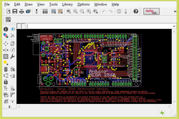
Creating layout
Once your schematic is ready and you start making PCB layout for this technique you have to take care that your PCB design must not exceed the maximum printer page sizes. To use this technique your PCB designs track width must not be too thin you have to use moderate track widths. once your PCB design is ready you have to simply print this PCB layout on a standard photo paper with any laser printer most preferably used black and white printers do not use color ink printers and while printing print only one layer at a time do not print all the layers at once. Print only copper tracks from the bottom layer of PCB.
Now carefully check the print for any variations or any misprint once you are sure that your print is perfect then take a copper clad PCB and clean the copper areas surfaces. any contaminations on the copper area must be cleaned using normal tap water do not use any kind of washing soda or any washing Chemicals.
Transfer
Take the printed paper and cut it to the size of PCB.
Place this paper on the copper layer facing printed area towards the copper surface.
Use document laminator and Pre heat it now pass the copper PCB and paper carefully through the laminator do not let them move while passing through the laminator. Carefully repeat this 2 to 3 times until the paper completely sticks on PCB now let the PCB cool down. if you don't have a Laminator then you can use electric iron. Heat the iron to its maximum setting, once it's hot, carefully place the paper on PCB same as for laminator and rub hot iron on the white, nonprinted side of the paper. and rub it till the paper is completely stick to the PCB. it will take 10 to 20 minutes to stick completely stick the paper on PCB let the paper turn slightly Brown now you are ready to take the paper out. let the PCB cool down to normal temperature room temperature. do not add water to cool.Once PCB is cooled carefully try to remove the paper from PCB surface you will see all the black ink from the paper is now on the copper surface and remaining paper will come out so now you have your PCB layout on the copper surface.
Carefully check the PCB layout for any cracks or miss print if you find any crack or miss print repair it with any oil based paint. the best way is to use high-quality permanent marker pens once you confirm that layout is ok you are ready for next stages.
Etching
For etching, you have to purchase Chemicals like ferric chloride or sodium persulphate from your local chemical store.
You can use any plastic container for this process. dip the PCB in the container with the etching solution and let the exposed copper dissolve in the chemical. it will take about half an hour to completely dissolve the remaining copper in your etching solution. Keep checking time to time until you see a finished PCB tunnecessary copper is removed take out the PCB clean it with normal tap water and then use a kitchen scrubber to remove black ink from the copper surfaces now you will see a fully finished PCB. now you can go for drilling and mounting components.
Comments
Post a Comment