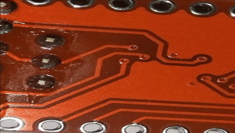
32 Layer PCB
A 32 Layer PCB is simply a multilayer PCB that has 32 layers sandwiched together to function as one PCB. Manufacturing this kind of PCB cannot be done using the conventional PCB Etching methods. This is because of the high precision expected. Advanced PCB Manufacturing methods are employed to ensure high quality and low electromagnetic radiation in the produced PCBs.
Preparing a Multilayer Layer PCB
Every professional PCB Design starts with a software design. The software design is the PCB Layout that give rise to Gerber files and Drill files; which are very useful in PCB Fabrication. The on-board electronics are then assembled by an automated pick and place robot. For a 32 Layer PCB, assembly details are not only specified in the normal Bill of Materials (BOM) PCB Design files. A separate file containing a set of assembly instructions must accompany the software design files.
Technique Behind 32 Layer PCB
To manufacture a 32 Layer PCB, a Stack-Up made up of multiple PCB layers is constructed. This is made possible by the machine; sandwiching multiple double layer PCBs with the help of an insulating fiber-epoxy layer in between every two double layer PCB. This insulating material is also called prepreg. This implies that the basic building blocks of any multilayer PCB is a double layer PCB. With this two-sided PCB fabrication technique at hand, and with more advanced machines to handle the increased complexity, fabrication of a 32 Layer or even a 50 Layer PCB is well achievable.
32 Layer PCB Applications
Why do we need these 32 or 50 Layer PCBs? One of the obvious reasons is to efficiently embed all the required system electronics in one small sized PCB. Even though components assembly is dedicated to top and bottom layers, it is possible to have components in between the Stack-up. Aerospace industry does a good job in making these complex PCB designs. In any aerospace system, the target is to have very little or no electromagnetic emission as possible. Organizing a PCB during the design phase does a great job in arresting these emissions. Each PCB layer is usually dedicated to a certain function which is not conflicting with other layers. For example, middle layers could be used as supply power planes, while top and bottom layers are set aside for component placement.
Comments
Post a Comment