Abstract
Producing a printed circuit board on a scale requires higher efficiency to counteract the cost of manufacturing in total. The major post design aspect to consider during the design stage is the selection of PCB size and PCB panel size. Which is generally referred to as panelization.
Content
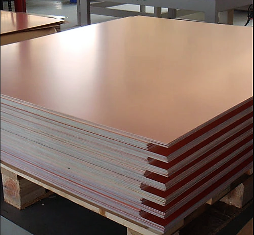
1.Standard PCB panel size
2.2 x 2 PCB panel size
3.PCB fabrication panel size
1.Standard PCB panel size
During the manufacturing stage fitting maximum number of layouts on a standard PCB panel size determines the effective use of the material. For example, in an 18"x24" PCB panel size fitting a two 8”x11” layout will yield an efficiency of roughly 80% but if the standard panel size is fitted with a two 8”x7” layouts will only yield an efficiency of roughly 30%. The efficiency of the production also depends on various other factors like type of breakout and border clearance. Although some manufacturers stick to producing their own panel size the rest stick to the standard PCB panel size as this makes easy to configure the boards in a automated production and assembly line and cost the PCB panel is considerably lesser.
2.2 x 2 PCB panel size
Usage of the 2”x2” PCB panel size eliminates the need of the panelization for the smaller board requirements. Fitting the layout on a predetermined size will reduce the cost of the production. The standard sizes can be quoted form the manufacturer for the design optimization. The board size and the designed layout must have a considerable ratio to keep up the efficiency. Dividing a larger panel size into a huge number of smaller layouts will plummet the efficiency.
3.PCB fabrication panel size
PCB panelization efficiency will also depend on the breakout type. V-cut and perforated tabs are most commonly used breakout methods. Although both of them need precise routing and border clearance they have the different take on efficiency depending on the board size. On a typical standard panel size, most commonly 18” × 24”. In which a ½” border clearance is required for handling the panels when processing boards and this clearance increase with increase in layers typically an inch for multilayer boards. Apart from the border clearance, milling clearance in the range of 0.1”to 0.5” has to be provided for the V and perforated holes. This all fits for the identical boards that is being manufactured but for non-identical and prototype boards panelization process is much more tedious due to the risk of manually fixing the strategic position.

Comments
Post a Comment